
Punjab State Board PSEB 12th Class Physics Important Questions Chapter 14 Semiconductor Electronics: Materials, Devices and Simple Circuits Important Questions and Answers.
PSEB 12th Class Physics Important Questions Chapter 14 Semiconductor Electronics: Materials, Devices and Simple Circuits
Very short answer type questions
Question 1.
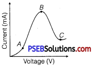
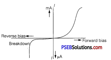
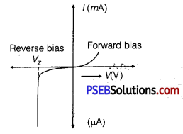
The graph shown in the figure represents a plot of current versus voltage for a given semiconductor. Identify the region at which 5 the semiconductor has a negative resistance.
Answer:
Resistance of a material can be found out by the slope of the curve V versus I. Part BC of the curve u shows the negative resistance as with the increase in current and decrease in voltage.
Question 2.
Sn, C, SI and Ge are all group 14 elements, Yet, Sn is a conductor, C is an insulator while Si and Ge are semiconductors. Why? (NCERT Exemplar)
Answer:
If the valence and conduction bands overlap (no energy gap), the substance is referred as a conductor. For insulators the energy gap is large and for semiconductors, the energy gap is moderate. The energy gap of Sn is O eV, for C is 5.4 eV, for Si is 1.1 eV and for Ge is 0.7 eV. Accordingly, their electrical conductivity varies.
Question 3.
Why are elemental dopants for Silicon or Germanium usually chosen from group 13 or group 15? (NCERTExemplar)
Answer:
The size of dopant atoms should be such as not to distort the pure semiconductor lattice structure and yet easily contribute a charge camer on forming covalent bonds with Si or Ge.
Question 4.
What happens to the width of depletion Layer of a p.n junction when it is
(i) forward biased,
(ii) reverse biased
Answer:
(i) When forward biased, the width of depletion layer decreases.
(ii) When reverse biased, the width of depletion layer increases.
![]()
Question 5.
In a transistor, doping level in base is increased slightly. How will it affect
(i) collector current and
(ii) base current?
Answer:
When doping level in base is increased slightly;
(i) Collector current decreases slightly and
(ii) Base current increases slightly.
Question 6.
Can the potential barrier across a p-n junction be measured by simply connecting a voltmeter across the junction (NCERT Exemplar)
Answer:
No, because the voltmeter must have a resistance very high compared to the junction resistance, the latter being nearly infinite.
Question 7.
Explain why elemental semiconductors cannot be used to make visible LEDs.(NCERT Exemplar)
Answer:
Elemental semiconductor’s band-gap is such that’ electromagnetic emissions are in infrared region.
Question 8.
Draw the logic circuit of a NAND gate and write its truth table.
Answer:
Logic circuit of a NAND gate

Truth table
| A | B | Y = A.B |
| 0 | 0 | 1 |
| 0 | 1 | 1 |
| 1 | 0 | 1 |
| 1 | 1 | 0 |
Short answer type questions
Question 1.
Write any two distinguishing features between conductors, semiconductors and insulators on the basis of energy band diagrams.
or
Draw the necessary energy band diagrams to distinguish between conductors, semiconductors and insulators. How does the change in temperature affect the behaviour of these materials? Explain briefly.
Answer:
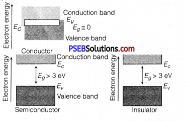
Distinguishing Features
(a) In conductors: Valence band and conduction band overlap each other.
In semiconductors: Valence band and conduction band are separated by a small energy gap.
In insulators: Valence band and conduction band are separated by a large energy gap.
(b) In conductors: Large number of free electrons are available in conduction band.
In semiconductors: A very small number of electrons are available for electrical conduction.
In insulators: Conduction band is almost empty i.e., no electron is available for conduction.
Effect of temperature
- In conductors: At high temperature, the collision of electrons become more frequent with the atoms/molecules at lattice site in the metals as a result the conductivity decreases (or resistivity increases).
- In semiconductors: As the temperature of the semiconducting material increases, more electron-hole pairs becomes available in the conduction band and valence band, and hence the conductivity increases or the resistivity decreases.
- In insulators: The energy band between conduction band and valence band is very large, so it is unsurpassable for small temperature rise. So, there is no change in their behaviour.
Question 2.
Distinguish between ‘intrinsic’ and ‘extrinsic’ semiconductors?
Answer:
| Intrinsic semiconductor | Extrinsic semiconductor |
| 1. It is a pure semiconductor material with no impurity atoms in it. | It is prepared by doping a small quantity of impurity atoms to the pure semiconductor. |
| 2. The number of free electrons in the conduction band and the number of holes in valence band is exactly equal. | The number of free electrons and holes is never equal. There is an excess of electrons in n-type semicoñductors and excess of holes in p-tpe semiconductors. |
Question 3.
The circuit shown in the figure has two oppositely connected ‘ ideal diodes connected in parallel. Find the current flowing through each diode in the circuit.
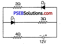
Answer:
(i) Diode D1 is reverse biased, so it offers an infinite resistance. So, no current flows in the branch of diode D1.
(ii) Diode D2 is forward biased and offers no resistance in the circuit. So, current in the branch,
I = \(\frac{V}{R_{e q}}=\frac{12 \mathrm{~V}}{2 \Omega+4 \Omega}=\frac{12 \mathrm{~V}}{6 \Omega}\) = 2A.
![]()
Question 4.
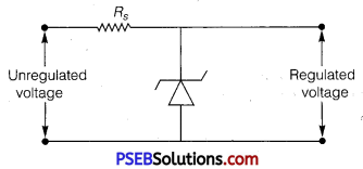
A Zener of power rating 1W is to be used as a voltage regulator. If Zener has a breakdown of 5V and it has to regulate voltage which fluctuated between 3V and 7 V, what should be the value of Rs for safe operation (see figure)? (NCERT Exemplar)
Answer:
Here, P =1W, Vz = 5 V
Vs = 3V to 7 V
IZmax = \(\frac{P}{V_{Z}}=\frac{1}{5}=0.2 \mathrm{~A}\) = 200 mA
Rs = \(\frac{V_{s}-V_{z}}{I_{Z_{\max }}}=\frac{7-5}{0.2}=\frac{2}{0.2}\) = 10Ω
Question 5.
Draw V-I characteristics of a p-n junction diode. Answer the following questions, giving reasons:
(i) Why is the current under reverse bias almost independent of the applied potential upto a critical voltage?
(ii) Why does the reverse current show a sudden increase at the critical voltage?
Name any semiconductor device which operates under the reverse bias in the breakdown region.
Answer:
(i) In the reverse biasing, the current of order of μA is due to movement/drifting of minority charge carriers from one region to another through the junction. A small applied voltage is sufficient to sweep the minority charge carriers through the junction. So, reverse current is almost independent of critical voltage.
(ii) At critical voltage (or breakdown voltage), a large number of covalent bonds break, resulting in the increase of large number of charge carriers. Hence, current increases at critical voltage. Semiconductor device that is used in reverse biasing, is Zener diode.
Question 6.
How is a light-emitting diode fabricated? Briefly state its working. Write any two important advantages of LEDs over the conventional incandescent low power lamps.
Answer:
LED is fabricated by:
(i) heavy doping of both the p and n regions.
(ii) providing a transparent cover so that light can come out.
Working: When the diode is forward biased, electrons are sent from n →b p and holes from p → n. At the junction boundary, the excess minority carriers on either side of junction recombine with majority carriers. This releases energy in the form of photon hv = Eg
Advantages:
- Low operational voltage and less power consumption.
- Fast action and no warm-up time required.
- Long life and ruggedness.
- Fast on-off switching capability.
Question 7.
Explain, with the help of a circuit diagram, the working of a photodiode. Write briefly how it is used to detect the optical signals.
Or
(a) How is photodiode fabricated?
(b) Briefly explain its working. Draw its VI characteristics for two different intensities of illumination.
Or
With what considerations in view, a photodiode is fabricated?
State its working with the help of a suitable diagram.
Even though the current in the forward bias is known to be
more than in the reverse bias, yet the photodiode works in reverse bias. What is the reason?
Answer:
A photodiode is fabricated using photosensitive semiconducting material with a transparent window to allow light to fall on the junction of the diode.
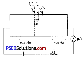
Working: In diode (any type of diode), an electric field ‘E’ exists across the junction from n-side to p-side, when light with energy hv greater than energy gap E2 (hv> Eg ) illuminate the junction, then electron-hole pairs are generated due to absorption of photons, in or near the depletion region of the diode. Due to existing electric fIeld, electrons are collected on n-side and holes are collected on p-side, giving rise to an emf. Due to the generated emf, an electric current of μA order flows through the external resistance.
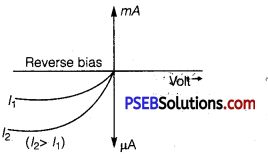
Detection of Optical Signals: It is easier to observe the change in the current with change in the light intensity if a reverse bias is applied. Thus, photodiode can be used as a photodetector to detect optical signals. The characteristic curves of a photodiode for two different illuminations I1 and I2 (I2 > I1)are shown below
Question 8.
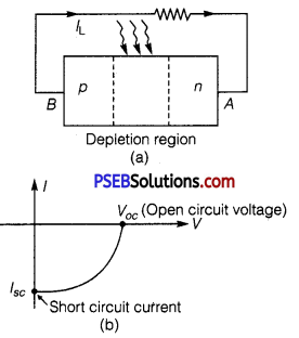
Describe briefly using the necessary circuit diagram, the three basic processes which take place to generate the emf in a solar cell when light falls on it. Draw the V-I characteristics of a solar cell. Write two important criteria required for the selection of a material for solar cell fabrication.
Answer:
The three basic processes which take place to generate the emf in a solar cell are generation, separation and collection.
(i) Generation of electron-hole pairs due to the light incident (with hv>Eg) close to the junction.
(ii) Separation of electrons and holes due to the electric field of the depletion region.
(iii) Collection of electrons and holes by n-side and p-side, respectively.
Important criteria for the selection of a material for solar cell fabrication are:
(i) bandgap (~ 1.0 to 1.8 eV).
(ii) high optical absorption (-10 4 cm-1),
(iii) electrical conductivity.
(iv) availability of the raw material, and
(v) cost
![]()
Long answer type questions
Question 1.
(a) State briefly the process involved in the formation of p-n junction explaining clearly how the depletion region is formed.
(b) Using the necessary circuit diagrams, show how the V-I characteristics of a p-n junction are obtained in:
(i) Forward biasing
(ii) Reverse biasing
How are these characteristics made use of in rectification?
Or
Draw the circuit arrangement for studying the V-I characteristics of a p-n junction diode
(i) in forward bias and
(ii) in reverse bias. Draw the typical V-I characteristics of a silicon diode.
Describe briefly the following terms:
(i) “minority carrier injection” in forward bias
(ii) “breakdown voltage” in reverse bias.
Answer:
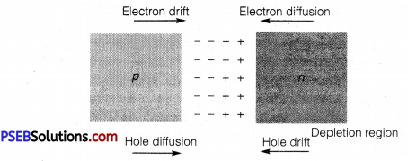
(a) Two processes occur during the formation of a p-n junction are diffusion and drift. Due to the concentration gradient across p and n-sides of the junction, holes diffuse from p-side to n-side (p → n) and electrons diffuse from n-side to p-side (n → p). This movement of charge carriers leaves behind ionised acceptors (negative charge Φ -immobile) on the p-side and donors (positive charge immobile) on the n-side of the junction. This space charge region on either side of the junction together is known as depletion region.
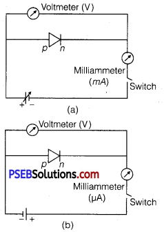
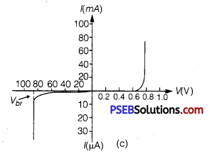
(b) The circuit arrangement for studying the V-I characteristics of a diode are shown in figure (a) and (b). For different values of voltages, the value of current is noted. A graph between V and I is obtained as in figure (c). From the V-I characteristic of a junction diode, it is clear that it allows current to pass only when it is forward biased. So, if an alternative voltage is applied across a diode, the current flows only in that part of the cycle when the diode is forward biased. This property is used to rectify alternating voltages.
(i) Minority Carrier Injection: Due to the applied voltage, electrons from n-side cross the depletion region and reach p-side (where they are minority carriers). Similarly, holes from p-side cross this junction and reach the n-side (where they are minority carriers). This process under forward bias is known as minority carrier injection.
(ii) Breakdown Voltage: It is critical reverse bias voltage at which current is independent of applied voltage.
Question 2.
State the principle of working of p-n diode as a rectifier. Explain with the help of a circuit diagram, the use of p-n diode as a full-wave rectifier. Draw a sketch of the input and output waveforms.
Or
Draw a circuit diagram of a full-wave rectifier. Explain the working principle. Draw the input/output waveforms indicating clearly, the functions of the two diodes used.
Or
With the help of a circuit diagram, explain the working of a junction diode as a full-wave rectifier. Draw its Input and output waveforms. Which characteristic property makes the junction diode suitable for rectification?
Answer:
Rectification: Rectification means conversion of AC into DC. A p-n diode acts as a rectifier because an AC changes polarity periodically and a p-n diode allows the current to pass only when it is forward biased. This makes the diode suitable for rectification.
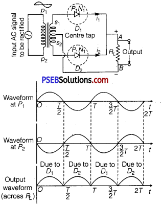
Working: The AC input voltage across secondary s1 and s2 changes polarity after each half cycle. Suppose during the first half cycle of input AC signal, the terminal S1 is positive relative to centre tap O and s2 is negative relative to O. Then diode D1 is forward biased and diode D2 is reverse biased. Therefore, diode D1 conducts while diode D2 does not. The direction of current (i1) due to diode D1 in load resistance RL is direction from A to B. In next half cycle, the terminal s1 is negative and s2 is positive relative to centre tap O.
The diode D1 is reverse biased and diode D2 is forward biased. Therefore, diode D2 conducts while D1 does not.
The direction of current (i2) due to diode D2 in load resistance RL is still from A to B. Thus, the current in load resistance RL is in the same direction for both half cycles of input AC voltage. Thus for input AC signal the output current is a continuous series of unidirectional pulses. In a full-wave rectifier, if input frequency is f hertz, then output frequency, will be 2f hertz because for each cycle of input, two positive half cycles of output are obtained.
Question 3.
Why is a Zener diode considered as a special purpose semiconductor diode? Draw the I-V characteristics of Zener diode and explain briefly, how reverse current suddenly Increase at the breakdown voltage? Describe briefly with the help of a circuit diagram, how a Zener diode works to obtain a constant DC voltage from the unregulated DC output of a rectifier.
Answer:
Zener diode works only in reverse breakdown region that is why it is, considered as a special purpose semiconductor. I – V characteristics of Zener diode is given below.
Reverse current is due to the flow of electrons from n → p and holes from p → n. As, the reverse-biased voltage increase the electric field across the junction, increases significantly and when reverse bias voltage V = VZ, then the electric field strength is high enough to pull the electrons from p-side and accelerated it to n-side. These electrons are responsible for the high current at the breakdown.
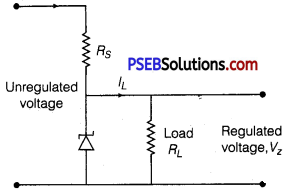
Voltage regulator converts an unregulated DC output of rectifier into a constant regulated DC voltage, using Zener diode. The unregulated voltage is connected to the Zener diode through a series resistance Rs such that the Zener diode is reverse biased. If the input voltage increase, then-current through Rs and Zener diode increases.
Thus, the voltage drop across Rs increase without any change in the voltage drop across zener diode. This is because of the breakdown region, Zener voltage remains constant even though the current through Zener diode changes.
Similarly, if the input voltage decreases, the current through Rs and Zener diode decreases. The voltage drop across Rs decreases without any change in the voltage across the Zener diode. Now, any change in input voltage results the change in voltage drop across Rs, without any changes; in voltage across the Zener diode. Thus, Zener diode acts as a voltage regulator.
![]()
Question 4.
(a) Differentiate between three segments of a transistor on the basis of their size and level of doping.
(b) How is a transistor biased to be in active state?
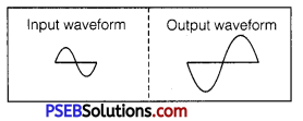
(c) With the help of necessary circuit diagram, describe briefly how n-p-n transistor in CE configuration amplifies a small sinusoidal input voltage. Write the expression for AC current gain.
Or
Explain with the help of a circuit diagram the working of n-p-n transistor as a common emitter amplifier.
Or
Draw the circuit diagram of a common-emitter amplifier using an n-p-n transistor. What is the phase difference between the input signal and output voltage? Draw the input and output waveforms of the signal. Write the expression for its voltage gain. State two reasons why a common emitter amplifier is preferred to a common base amplifier.
Answer:
(a) Emitter: It is of moderate size and heavily doped.
Base: It is very thin and lightly doped.
Collector: The collector side is moderately doped and larger in size as compared to the emitter.
(b) Transistor is said to be inactive state when its emitter-base junction is suitably forward biased and base-collector junction is suitably reverse biased.
(c) The circuit of common emitter amplifier using n-p-n transistor is shown below :
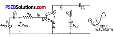
Working: If a small sinusoidal voltage, with amplitude VS is superposed on DC basic bias (by connecting the sinusoidal voltage in series with base supply VBB), the base current will have sinusoidal variations superimposed on the base current IB.
As a consequence the collector current is also sinusoidal variations superimposed on the value of collector current Ic, this will produce corresponding amplified changes in the value of output voltage V0.
The AC variations across input and output terminals may be measured by blocking the DC voltage by large capacitors. The phase difference between input signal and output voltage is 180°. The input and output waveforms are shown in figure.
Voltage gain,
Av = \(\beta \frac{R_{L}}{R_{i}}\)
AC current gain, βAC = \(\left(\frac{\Delta I_{C}}{\Delta I_{B}}\right)_{V_{C E}}\)
Reasons for Using a Common Emitter Amplifier
(i) Voltage gain is quite high.
(ii) Voltage gain is uniform over a wider frequency range or power gain is high.